
What's the REAL Secret to Becoming a TOP Hardware Engineer?
🛍️ Products Mentioned (1)
Get good at PCB design now, not later: https://academy.hasofu.com/course/hardware-engineer-accelerator-videos-group If you want to get good at PCB design in 3-4 months instead of 3-4 years, enroll in the Elite Hardware Engineer (PCB Design) Accelerator Program today. You will master the design of high-speed PCBs, expertly navigating Signal Integrity (SI), Power Integrity (PI), Electromagnetic Compatibility (EMC), and Electromagnetic Interference (EMI) constraints. Summary We will help you unlock your inner potential so you can excel in your professional field. Some of the benefits of our trainings are: Foundations of PCB Design - Build your first 2-layer PCB from start to finish (M)anufacturing and Excellence in Design - Build your second 2-layer PCB from schematic to PCB based on IPC-2221 and our proprietary PCB design processes (E)lectromagnetism (EMI, EMC, ESD) - Learn the foundations of Electromagnetism from an intuitive approach to PCB design (S)ignal Integrity Essentials - Learn all root problems of signal integrity and how to remove them for good - Build a 10-layer board (H)igh-Speed Digital Design - Learn high-speed digital design and Build your first high-speed practical PCB at 10 Gbps - xnets, diffpairs, tuning, length matching, etc. Power Integrity (PI) - Power Distribution Network Design - Bring it all together by designing a power electronic board and reduce impedance profile and more... Course Content: MODULE 1: INTRODUCTION (Reading Requirements) Learn about Design for Manufacturing, Signal Integrity, Electromagnetic Interference, and High-Speed Digital Design Understand the PCB designer’s journey on the job Assigned Reading to Understand the full PCB Design process MODULE 2: PROJECT 1 – DESIGN A PCB IN 2 HOURS TO UNDERSTAND PCB DESIGN SOFTWARE Schematic Capture PCB Overview, Stack-up and Setup, Creation Component Placement, Design Rules, Part Placement, Routing, Routing Clean-up Manufacturing Preparation, Creating Design Outputs for Manufacturing – Gerber & Drill Design Review Software navigation, process, procedure Understand manufacturing, stack-up, high-speed concepts, and standards MODULE 3: DESIGN FOR MANUFACTURING – PROJECT 2 SCHEMATIC CAPTURE Learn the HaSofu Academy Kirsch Mackey’s MESH Design Process The Design for Excellence Process (Manufacturing, Fabrication, Assembly & Test) DESIGN FOR Excellence (DFx) – PROJECT 2 PCB LAYOUT PCB Stack-up from the Manufacturer, PCB Board Outline from DXF Import & Mounting Hole Creation Apply Fabrication Design Rules, Shortcuts for improved PCB design efficiency Understand Return Paths in Mixed-signal PCB design (Signal Integrity) Component placement, Design Sync (Engineering Change Orders) Creating Design for Assembly Rules, Collision Detection and Visualization Manufacturing Test Points, Routing and Copper Pour for Ground and Power, Mixed Signal Layout Differential pair routing, Design rules check, 3D MCAD Model Exports Packaging and sending Manufacturing Deliverables MODULE 6: MULTILAYER PCB, SI & EMI + Schematic Design Reuse – PROJECT 3 SCHEMATIC CAPTURE Understand the nine key signal integrity issues and how to overcome them Circuit SPICE simulation for analog, digital analysis Advanced block diagram layout + floor planning for PCB Part organization, time efficiency, Net names / aliases, Design rules check Bill of Materials, PCB Trace Current Carrying capacity calculation, PCB Trace voltage withstanding clearance MODULE 7: MULTILAYER STACK-UP ANALYSIS FOR SIGNAL INTEGRITY AND EMI (PROJECT 3 PCB LAYOUT) Learn to design with signal integrity and EMI considerations embedded into design habits Analysis of 4-layer, 6-layer, 8-layer, and 10-layer PCB stack-ups Assignments to assess all the layer types, project-specific stack-up for Dual Rail Power Supply Design (10 layers) MODULE 8: MULTILAYER DESIGN FOR SI, EMI, EMIC – PROJECT 3 CONTINUED Solve each of the signal integrity and EMI problems while building a design Mounting Holes, Part Placement, Custom Colors, Exporting Design constraints, Blind and Buried VIAs setup Fixing Signal Reflections, Crosstalk, VIA Stubs, Skew, Signal Attenuation, Ground Bounce Power, Ground, Critical Net, and Length Matching routing Grounding shield, more... MODULE 9: INTRODUCTION TO HIGH-SPEED DIGITAL DESIGN - USB-C PROJECT Introduction to HSDD concepts Part Selection, Materials for high-speed board stack-up Design a USB A to USB C converter for USB 3.2 Gen 1 (5 Gbps) from scratch Simulate the high-speed digital design response, Learn Length and phase tuning, propagation and speed delay, eye diagrams... More on the website...
🎬 More from TechEdKirsch

Hardware PCB design best practices for adding components (shown using Altium)
169 views

How Do Companies Create Hardware Products? Process Overview for Electrical Engineers
128 views
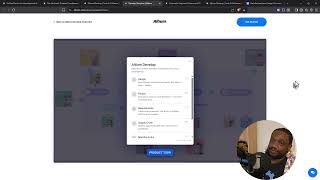
What is Altium Doing in 2026? Altium Develop and Agile The Best for Hardware Companies???
222 views
Altium Develop - Adding components to your workspace (for SMBs)
143 views
Altium Designer Tip - How to Make Pin Numbers Not Visible for Teams and Enterprise
48 views

Altium Designer Develop 2026 Part 1 - Installation and What is it?
481 views