
PCB Footprints Not Working in OrCAD? Top 3 Reasons Why | EE Nomad Life
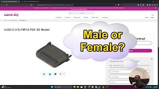
In this video I share how to properly understand Cadence OrCAD software so you can find the PCB footprints you're looking for. Know that it's more than you might think. Having in-depth knowledge of your PCB design software is critical to solving problems in industry. So in this video I get you up on game with how to understand how this powerful software works. 00:00 Intro 00:27 Who I am 01:30 OrCAD Footprints Common Problems 12:00 Advice for Computer Engineering Students and Electrical Engineers 13:15 How I Work as a Content Creator 13:50 Mistake I've Made as a Freelancer 14:35 What Problems Have you Run Into 14:50 How I'm able to travel + Benefits of Both sides 15:56 How to Live the Tech Nomad Life
🎬 More from TechEdKirsch
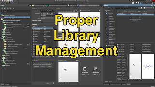
Hardware PCB design best practices for adding components (shown using Altium)
169 views

How Do Companies Create Hardware Products? Process Overview for Electrical Engineers
128 views
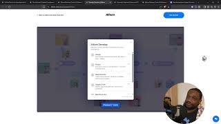
What is Altium Doing in 2026? Altium Develop and Agile The Best for Hardware Companies???
222 views
Altium Develop - Adding components to your workspace (for SMBs)
143 views
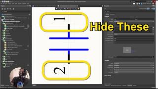
Altium Designer Tip - How to Make Pin Numbers Not Visible for Teams and Enterprise
48 views

Altium Designer Develop 2026 Part 1 - Installation and What is it?
481 views