
PCB Design for Industry - The 12 Phases
🛍️ Products Mentioned (2)
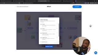
Download Altium Develop: https://www.altium.com/yt/kirschmackey Master hardware for industry: https://acadmey.hasofu.com/courses @AltiumStories #altiumstories 00:00 Intro 00:58 Phases 1 - Requirements (MOST IMPORTANT) 03:15 Phase 2 - Specifications - 4 04:24 Phase 3 - Library Management 05:23 Phase 4 - Schematic Design vs. Schematic Capture 06:38 Phases 5 & 6 07:37 Hardware Design Coaching 07:57 Phase 7 - PCB Routing 08:36 Phase 8 DRC Pre-route and Post-Route Verification (PCB Simulation), DFF, DFT, DFA 09:18 Phase 9 PCB Finalization 09:54 Phase 10 Manufacturing Files, Output Files, Ordering the PCB Assembly 10:35 Phase 11 Testing and Release 10:51 Production 11:49 Altium Develop Ever wonder how hardware and PCB design engineers create their own PCBs in industry? How it's done in corporate? the process is a lot more involved than you think. I'm showing you all the 12 phases of hardware and PCB design as a quick overview of what hardware and PCB designers check and perform from schematic design to PCB layout to manufacturing files (Gerber, etc.). Now I can't go into as much depth as I want to in this video, so I'll release videos in the future that get into each of the phases in greater detail.
About This Video
Frequently Asked Questions
🎬 More from TechEdKirsch
Hardware PCB design best practices for adding components (shown using Altium)
169 views

How Do Companies Create Hardware Products? Process Overview for Electrical Engineers
128 views
What is Altium Doing in 2026? Altium Develop and Agile The Best for Hardware Companies???
222 views
Altium Develop - Adding components to your workspace (for SMBs)
143 views
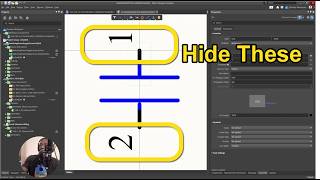
Altium Designer Tip - How to Make Pin Numbers Not Visible for Teams and Enterprise
48 views
Altium Designer Develop 2026 Part 1 - Installation and What is it?
481 views