
OrCAD23.1 How to Troubleshoot Flash Symbol Padstack Errors
🛍️ Products Mentioned (1)
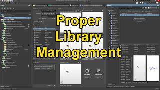
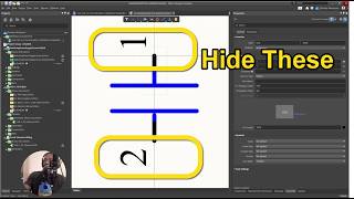
In this video you learn OrCAD 23.1 How to troubleshoot flash symbol padstack errors using the pad stack editor, PCB editor and OrCAD Capture. Learn more in the course: https://academy.hasofu.com/course/apple-hardware-engineer-accelerator We're updating the PCB footprints and padstacks of some older components from a PCB design project, the Beaglebone black. You will learn how to find the PCB footprint in OrCAD Capture, open it in OrCAD PCB Editor, update the padstack in pad stack editor, create multiple flash symbols in OrCAD 23.1, save them, then update the PCB footprint to clear the error. This is advanced component library training from the Electronics PCB Design course.
🎬 More from TechEdKirsch

Hardware PCB design best practices for adding components (shown using Altium)
169 views

How Do Companies Create Hardware Products? Process Overview for Electrical Engineers
128 views

What is Altium Doing in 2026? Altium Develop and Agile The Best for Hardware Companies???
222 views
Altium Develop - Adding components to your workspace (for SMBs)
143 views
Altium Designer Tip - How to Make Pin Numbers Not Visible for Teams and Enterprise
48 views

Altium Designer Develop 2026 Part 1 - Installation and What is it?
481 views