
Mastering PCB Stackups for Power Boards: Boost Converter Design & Common Mistakes Explained!
🛍️ Products Mentioned (3)
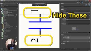
Altium + 365 free: http://altium.com/yt/techedkirschmackey Full Stack Hardware Engineer Mentorship: https://academy.hasofu.com/course/prohwe Mastering PCB Stackups for Power Boards: Boost Converter Design & Common Mistakes Explained! Want to design boards like a Professional? Enroll in the Elite Hardware Engineer Program: https://academy.hasofu.com/course/hardware-engineer-accelerator-videos-group In this video, I provide a detailed review and insights into PCB stackup considerations for power electronics design, specifically focused on a buck-boost converter. We explore dielectric thickness, plane-to-plane capacitance, EMI, and much more! Get ready for an in-depth look into designing efficient PCB layouts for power boards. Make sure to like, comment, and subscribe for more electronics engineering content! ⏱️ TIMESTAMPS: 0:00 - Introduction: Reviewing Ong's Project 5 - Overview of Buck-Boost Converter Design 0:07 - Acknowledgement & Video Scope 0:20 - Dielectric Thickness and Core Considerations 0:44 - Impact of Dielectric on Plane-to-Plane Capacitance 1:27 - Reducing Impedance and Signal Integrity 2:01 - Challenges with Core Separation and Capacitance 2:21 - EMI Concerns in Power Electronics 2:57 - Discussion on Foil, Prepreg, Solder Mask, and Copper Cores 3:12 - Layer Stackup Optimization 3:35 - Voltage and Ground Layer Strategies 4:12 - Capacitive Coupling and Trace Reduction 4:35 - Managing EMI with Inductor Placement 5:07 - Vias and Grounding for Inductors 5:24 - External vs. Internal Inductor Considerations 6:03 - Playing Capacitance and Adjusting Stackup Thickness 6:33 - VN and VBAT Trace Width Calculations 7:14 - Calculating Maximum Current for PCB Traces 7:33 - Trace Width Calculators & Standards 8:06 - Dielectric Thickness Impact on Impedance 8:20 - High-Speed Signal Considerations 8:40 - Managing Trace Impedance and Ground Distance 9:11 - Summary and Final Recommendations 💡 Related Topics Covered: PCB stackup design Power board layout tips Boost converter PCB considerations Capacitance and EMI in PCB design Dielectric thickness in PCB layers 👉 More PCB Design Content: How to Optimize PCB Layouts High-Speed Digital Design Tips PCB Design for Power Electronics 🔔 Subscribe for More Engineering Content! Like, comment, and let me know your questions or what you'd like to see next in the world of PCB design! #PCBDesign #BoostConverter #PowerElectronics #PCBStackup #ElectronicsEngineering #HighSpeedDesign #EMIManagement #CapacitanceOptimization
🎬 More from TechEdKirsch

Hardware PCB design best practices for adding components (shown using Altium)
169 views

How Do Companies Create Hardware Products? Process Overview for Electrical Engineers
128 views

What is Altium Doing in 2026? Altium Develop and Agile The Best for Hardware Companies???
222 views
Altium Develop - Adding components to your workspace (for SMBs)
143 views
Altium Designer Tip - How to Make Pin Numbers Not Visible for Teams and Enterprise
48 views

Altium Designer Develop 2026 Part 1 - Installation and What is it?
481 views